
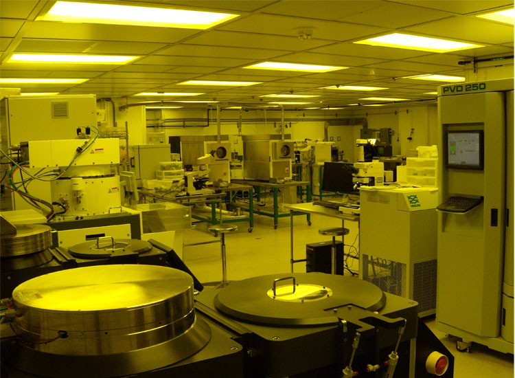
Listed below are the semiconductor processing and characterization facilities to which the Advanced Devices and Sustainable Energy Laboratory (ADSEL) group has access. The facilities are separated into three broad categories: growth and processing equipment, transport measurement equipment, and optical measurement equipment. In addition to the ADSEL owned facilities, the Virginia Tech associated facilities are listed towards the bottom. Clicking on an image thumbnail below will enlarge the image.
Electronic Materials Growth
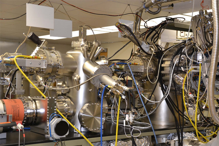
MBE Growth Facilities for Compound Semiconductors and Germanium-Tin
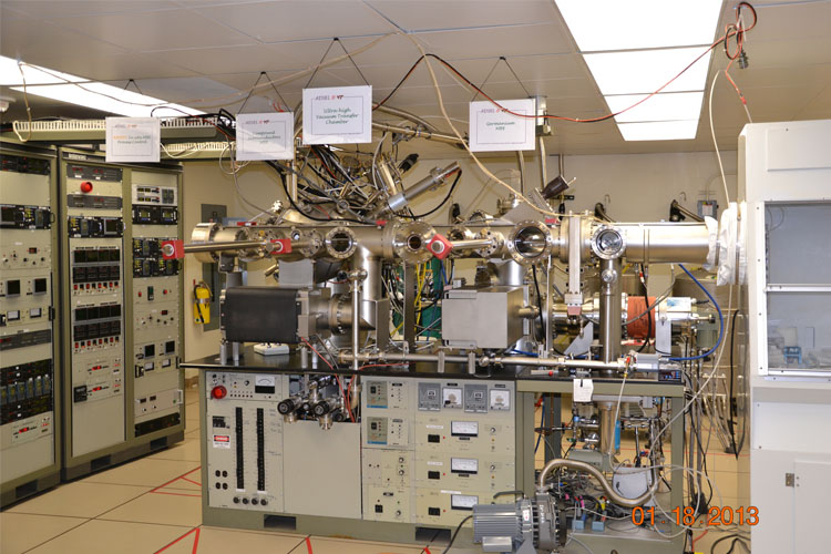
1. A dual chamber MBE growth facility for both group III-V and group IV (Ge, GeSn) connected by an ultra-high vacuum transfer chamber.
2. Group-III: Ga, In, Al; Group-V: As, Sb; Dopants: Si, Be, Te.
3. In-situ reflection high energy electron diffraction (RHEED) capability in order to:
- Analyze the initial surface pattern;
- Analyze surface reconstruction; and,
- Monitor the entire growth.
5. An optical IR pyrometer provides a real-time temperature feedback loop.
Solid Source Germanium MBE Growth Facility and Germanium SUMO cell
1. A solid source SUMO Ge cell for epitaxial Ge layer growth.
2. Allows for the growth rate and growth temperature to be precisely controlled during growth.
Antimony (Sb) Cracker for III-V MBE Growth Facility for mixed As-Sb based materials
Optical Microscope
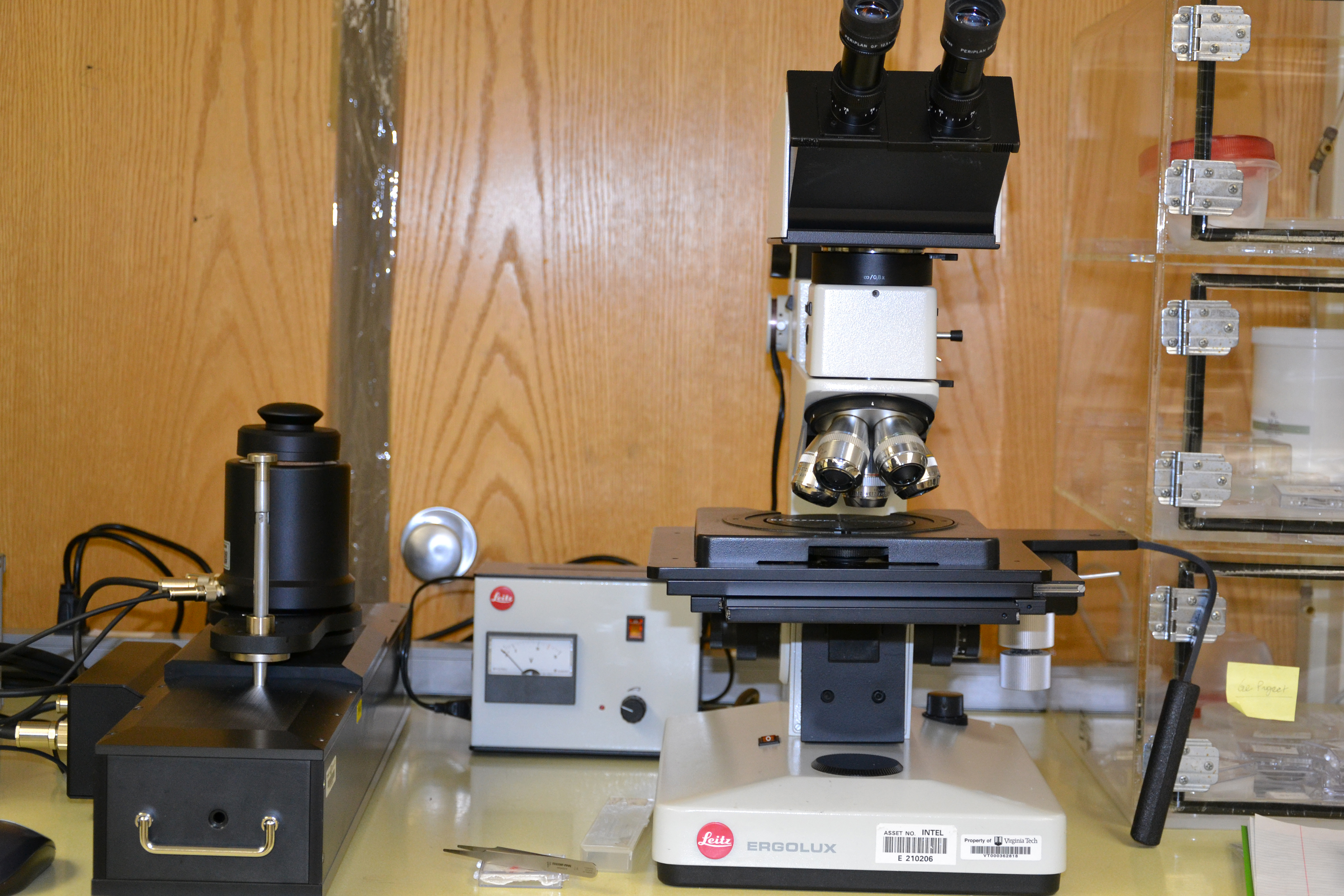
1. Leitz Ergolux optical microscope (donated by Intel) to inspect the surface defects or other features.
2. Allows to quick change of magnification during measurement.
Nomarski (Differential Interference Contrast) Microscope
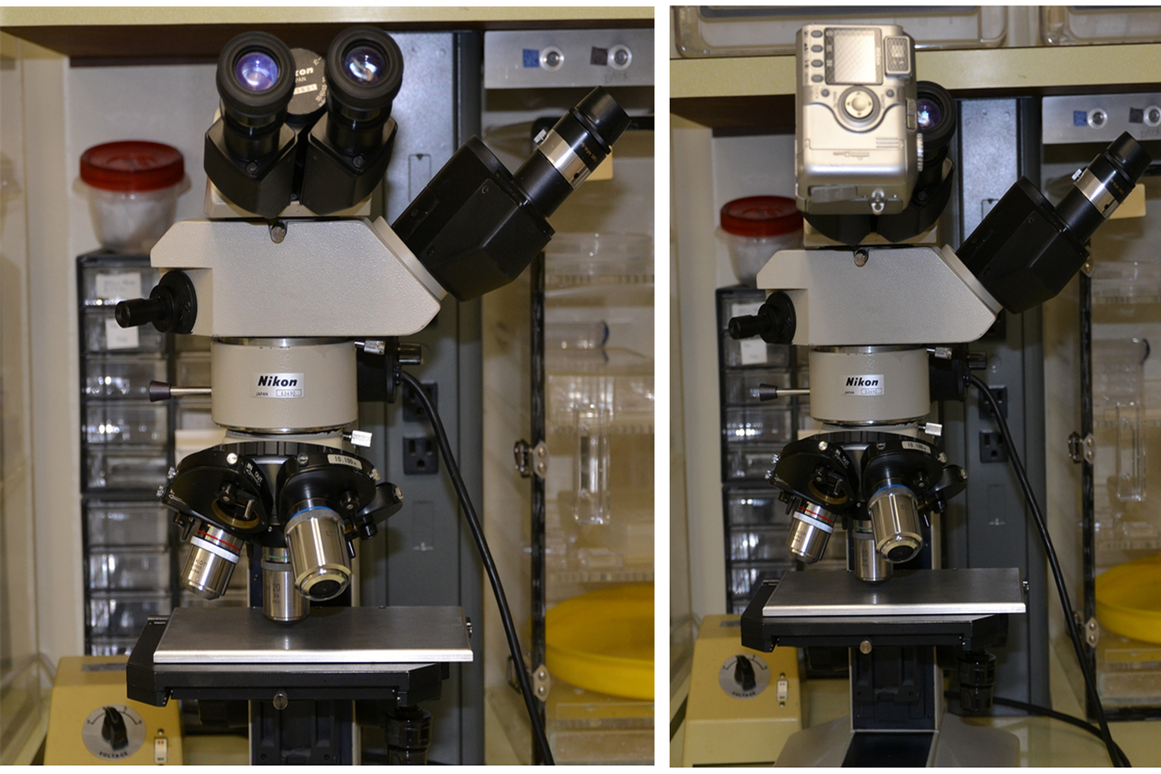
1. Nikon Optophot Nomarski microscope (Left) to inspect the surface defects or other features and surface cross-hatch pattern.
2. Attached Nikon digital camera (right) for capturing surface feature.
3. Additional attached eyepiece helped to realize two person observe the object at the same time.
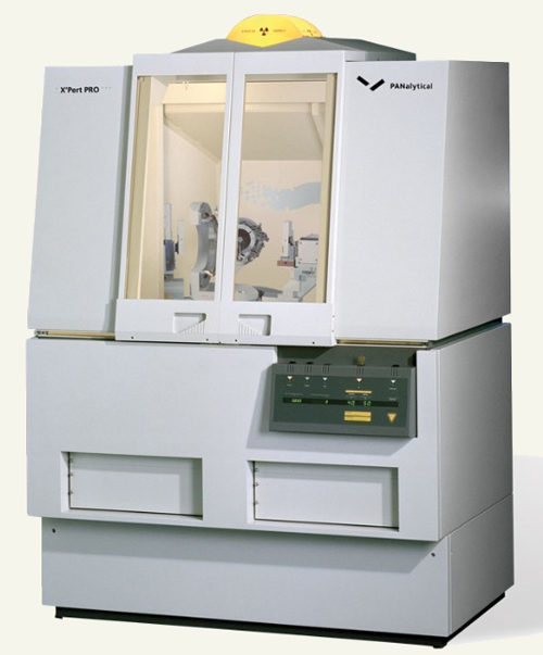
Panalytic X'pert Pro Triple Axis X-ray Diffractometer
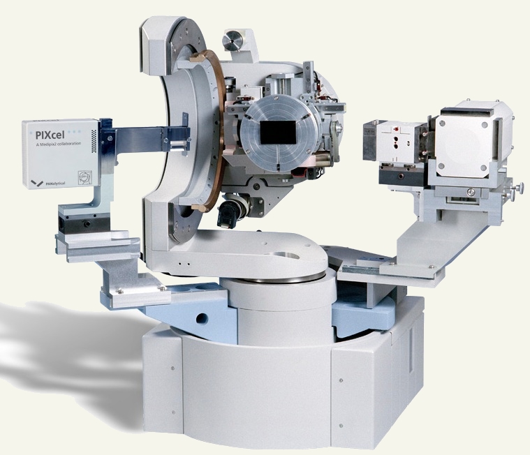
PIXcel Detector XRD System for Fast Reciprocal Space Mapping
Sample Preparation for Transmission Electron Microscopy
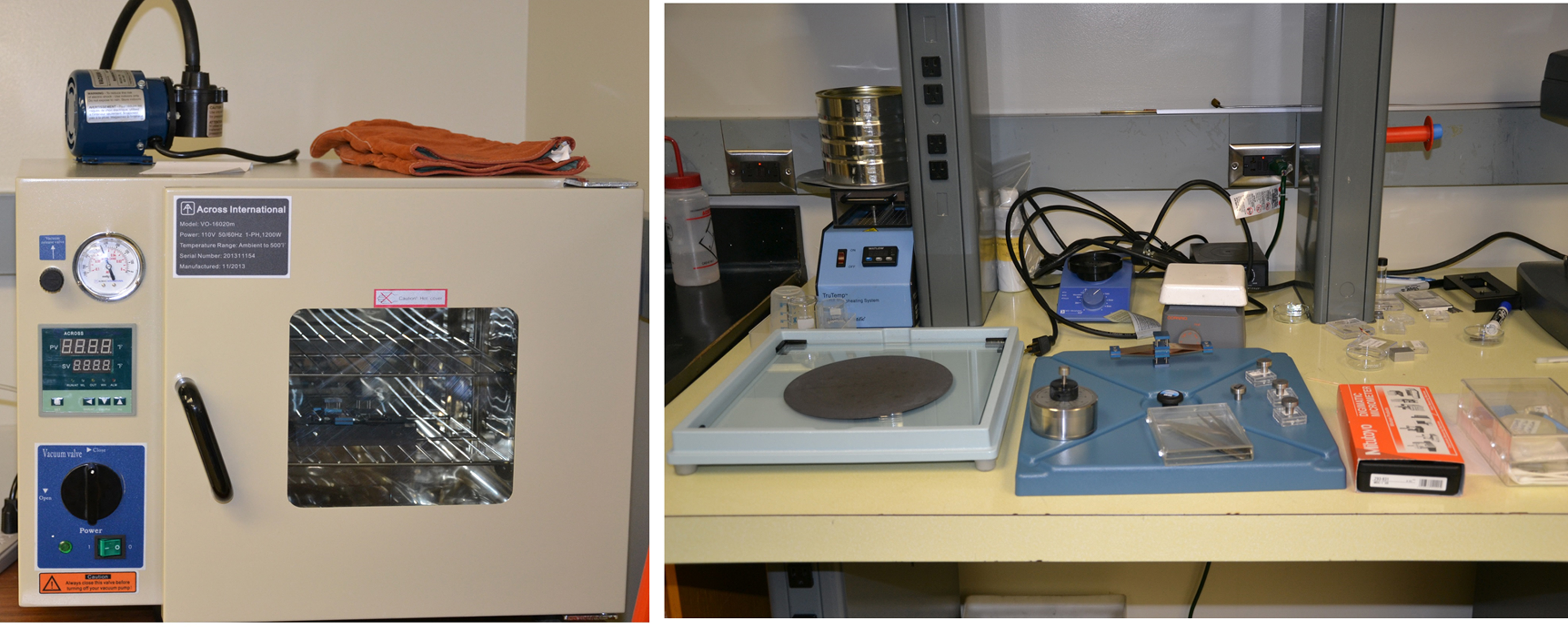
1. TEM furnace (Left) for bonding two samples fact-to-face.
2. Precision thickness control during sample polishing.
3. Thickness control down to about 20um prior to ion milling and TEM imaging.
Transport Measurement Facilities
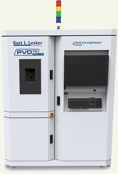
Contact Metal Deposition System
Thermolyne 21100 Tube Furnace for Contact Annealing
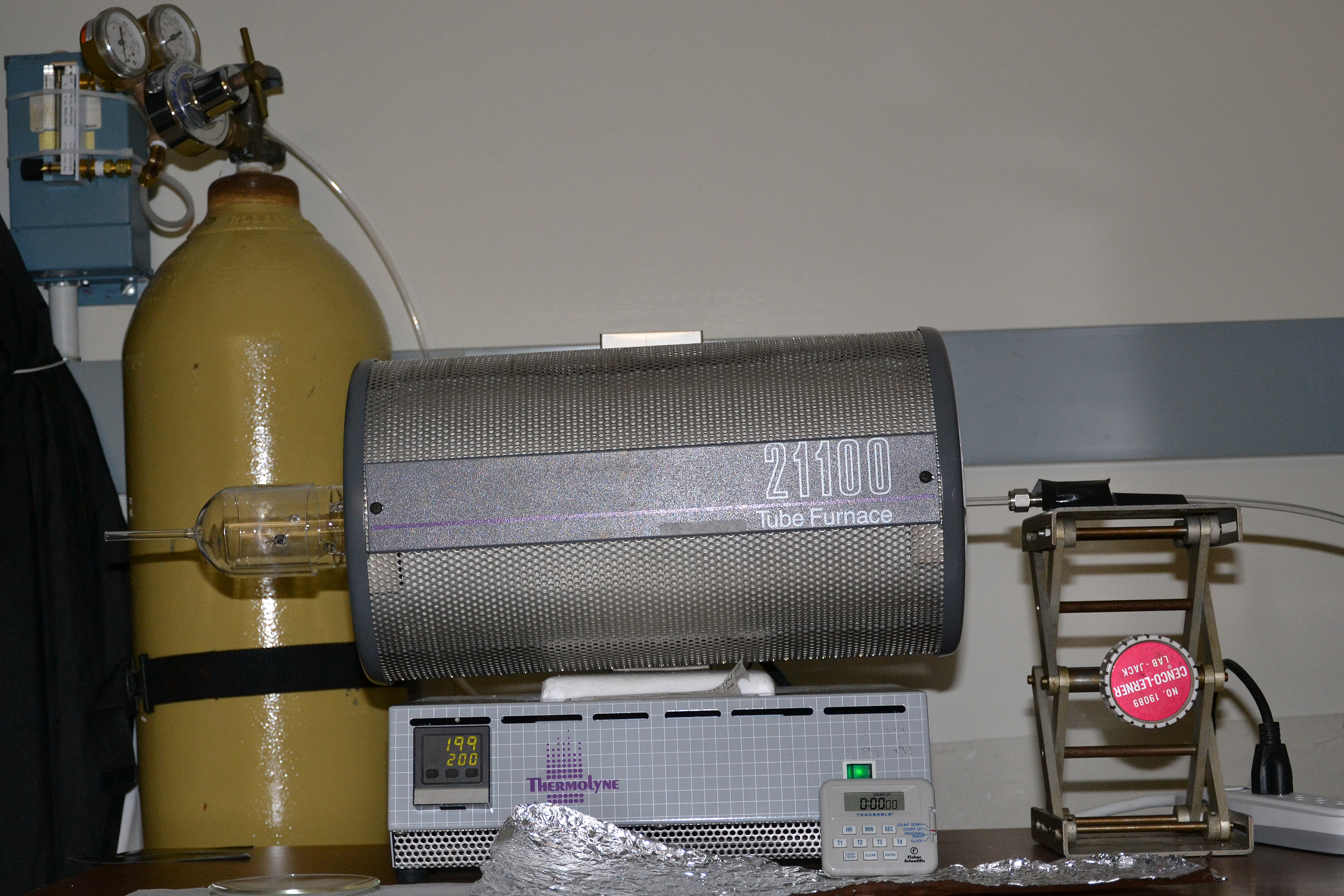
1. Contact annealing furnace to form Ohmic and Schottky contact.
2. Forming gas annealing of metal deposited contact to avoid oxygen exposure and superior ohmic contact for transport measurements.
3. Quartz tube and boat to avoid contamination and easy cleaning.
Temperature Dependent Hall Measurement System
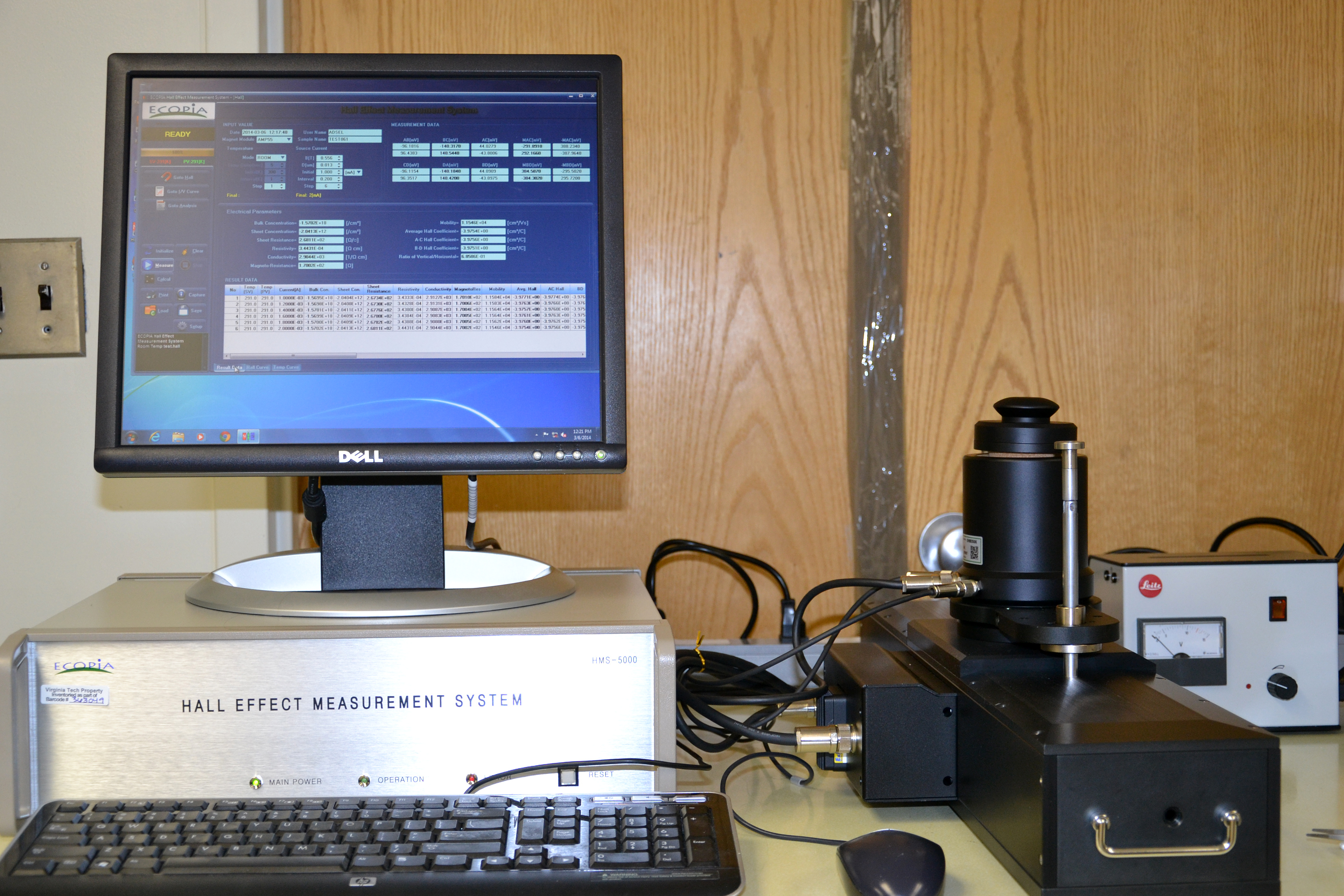
1. Ecopia temperature dependent (77K to 350K) Hall measure system.
2. Easy mounting of sample during measurement and not restricted by size of sample up to 1.5cmx1.5cm.
3. Fast measurement and data processing.
Advanced Research System Cryogenic Probe Station (Company photos, actual photos coming soon after installation)
Enable to perform I-V and C-V from liquid helium to 200oC temperature.
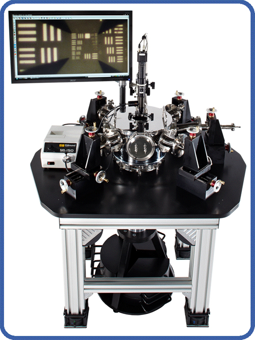
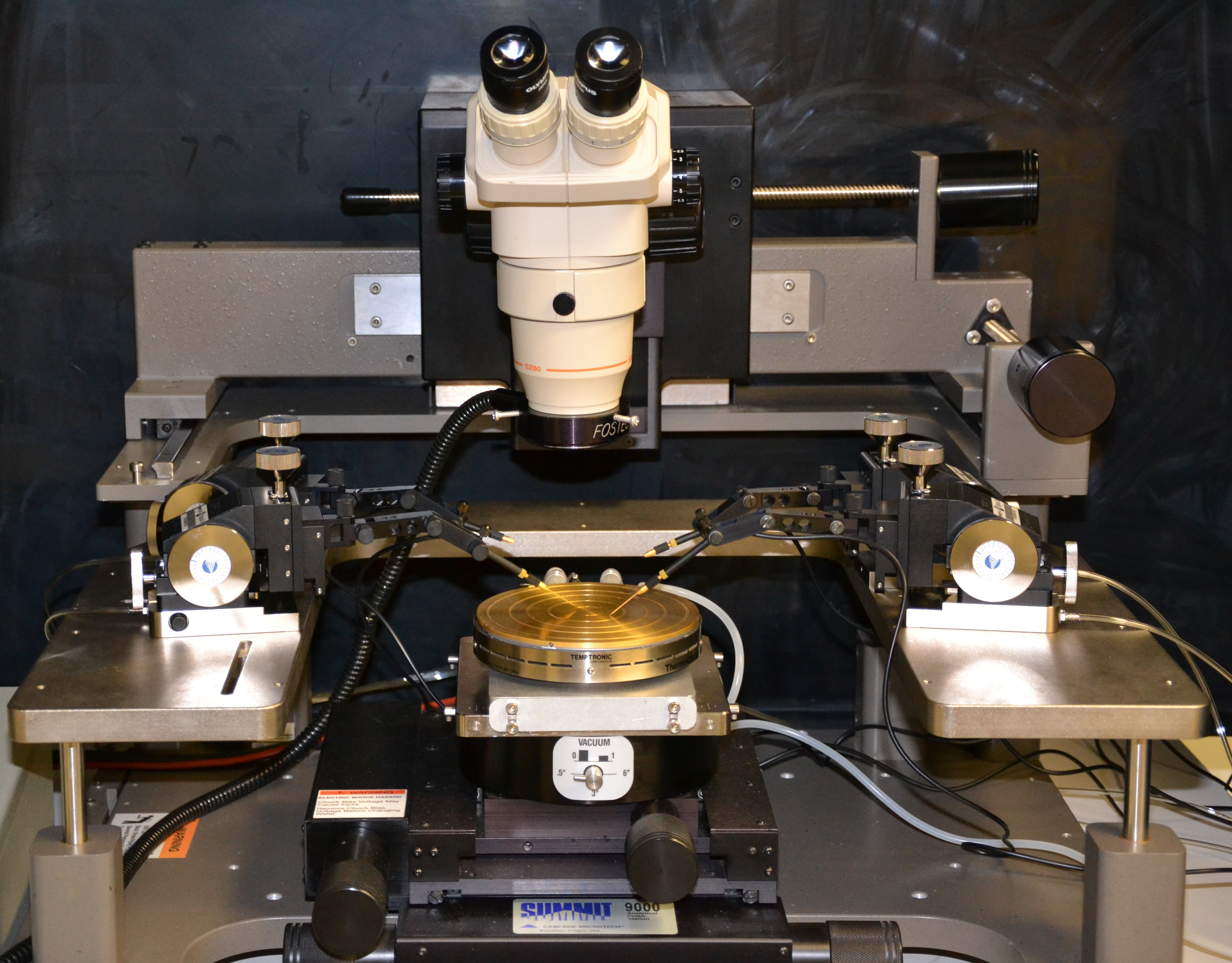
Integrated I-V, C-V, and G-V Characterization System with Cascade Summit 9000 Probe Station
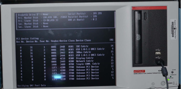
Keithley 4200-SCS Semiconductor Characterization System
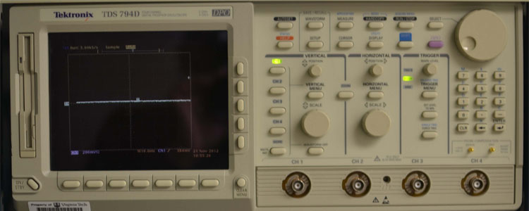
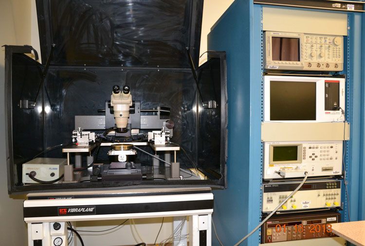
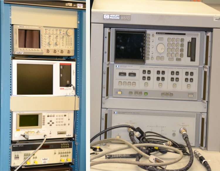
Pulse I-V/C-V Measurement (left) and HP 8510 Network Analyzer for RF Measurement (right)
Temperature Dependent (RT to 300C) Probe Station
Optical Measurement Facilities
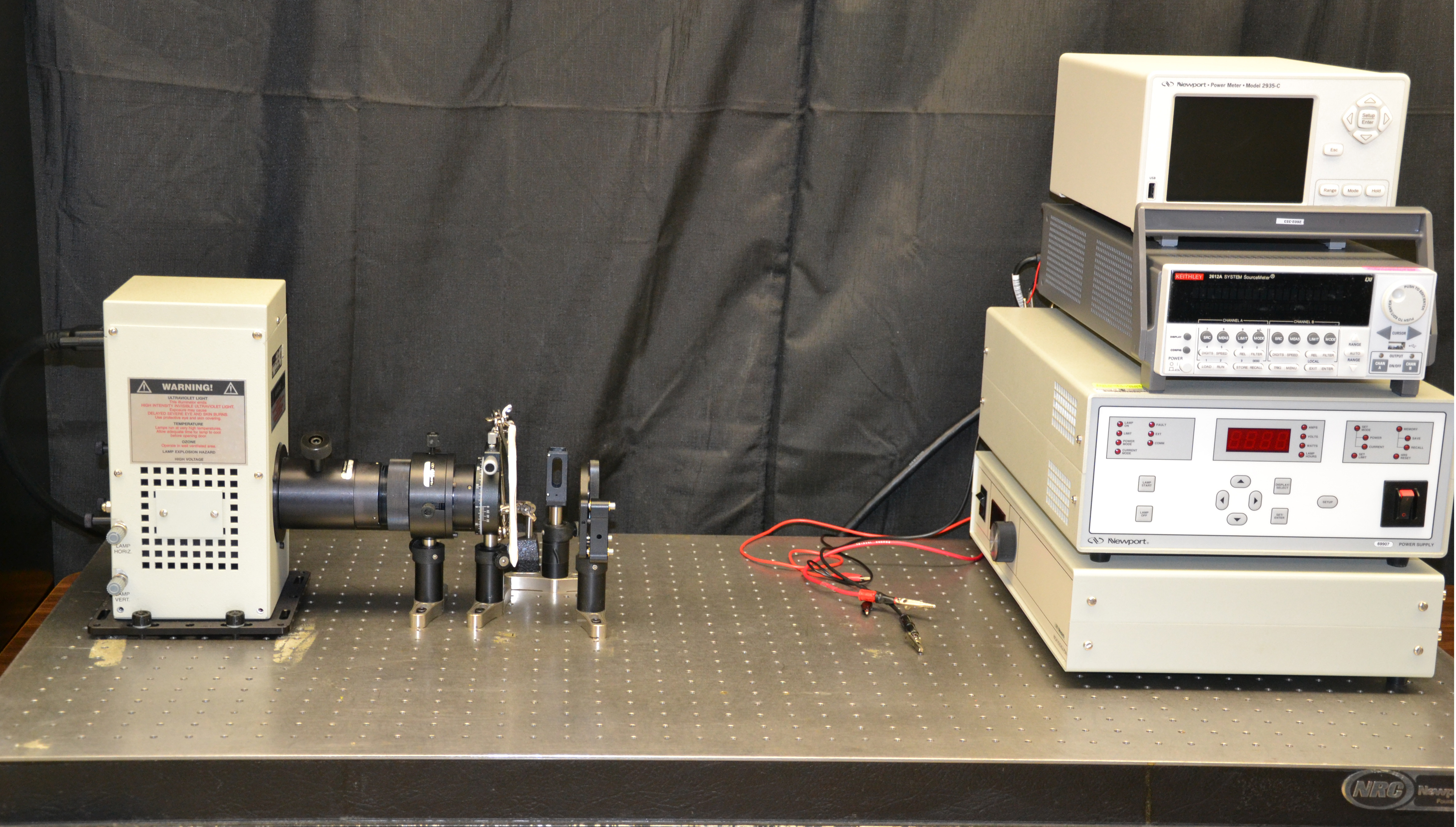
Fluorescence Spectroscopy (under construction)
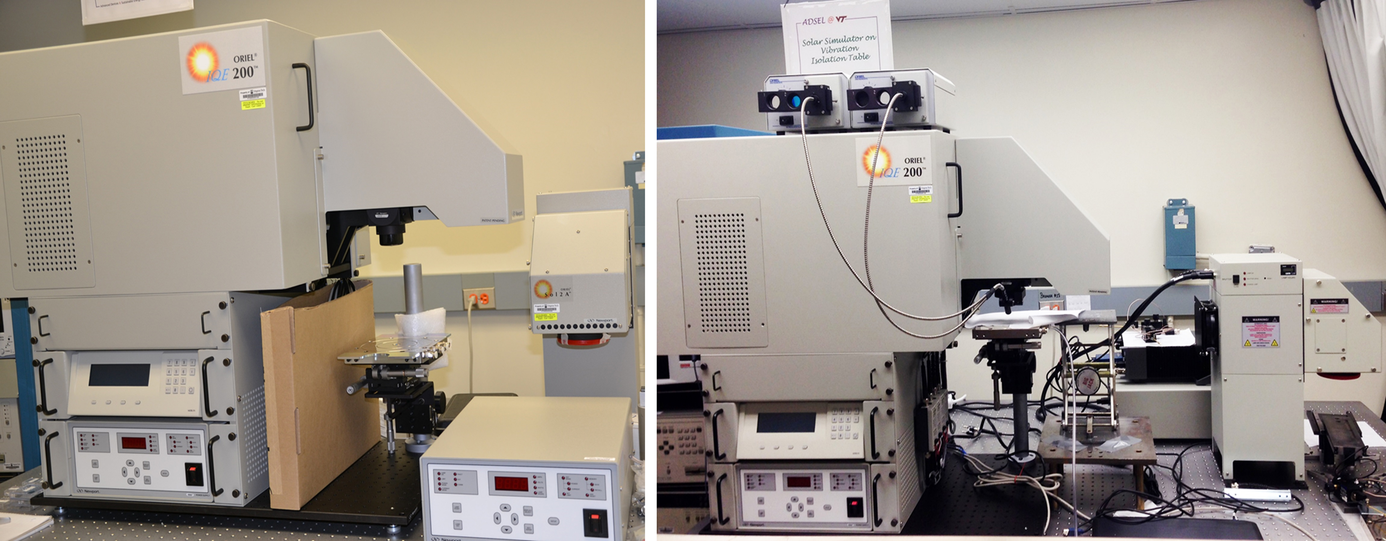
Solar Simulator and Oriel QE 200 System
Virginia Tech Associated Facilities
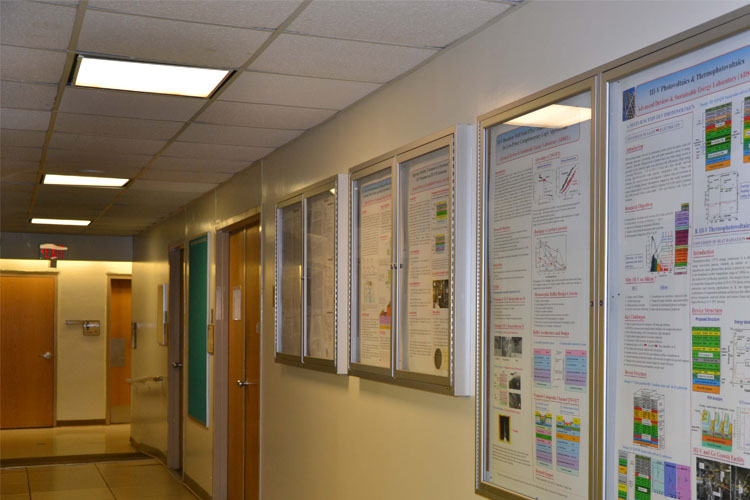
ADSEL Research Projects and Results Showcase